
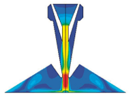
Conventional welding zone simulation comparing fusion zone size and shape
Welding is one of the oldest metal arts known to man. Additive manufacturing (or 3D printing) is one of the newest. Yet the two technologies have more in common than you might think. And few people understand this better than the experts at TWI (formerly The Welding Institute), established in Cambridge, UK in 1946.
TWI is one of the world’s foremost independent research and technology organisations, with expertise in materials joining and engineering processes as applied in industry. Its teams of consultants, scientists, engineers and support staff work with over 1,800 industrial members in 80 countries. Five UK and 13 overseas facilities serve both TWI members and some 25,000 students trained each year in welding and inspection technologies.
“Additive manufacturing can be thought of as a series of micro-welds,” describes Tyler London, regional team manager for TWI’s Numerical Modelling and Optimisation group. A chartered engineer, scientist, mathematician and professional simulation engineer, London has an MSc in mathematical modelling from Oxford and a background in offshore, aerospace and oil & gas fracture-integrity assessments. Simulation was a core tool during his student years and has proved particularly useful since he joined TWI in 2010 and began partnering with the additive manufacturing (AM) team.
“AM and welding are not very different in how one approaches their simulation,” he says. “Of course, the number of ‘microwelds’ in an AM simulation can be enormous, so simulation run times and memory become significant. But you are definitely investigating many similar phenomena in both technologies, such as phase transformations of metals, cooling rates, tool paths, residual stresses and distortion.”
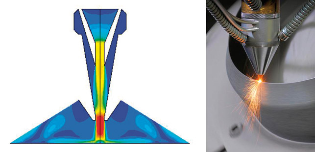
Thermal simulation used as input to Abaqus for multi-physics AM predictions of Laser Metal Deposition
TWI began working on computational weld modelling, with Simulia’s Abaqus software as its primary FEA tool, in the 1990s. It has deep expertise in material (constitutive) models, the modelling of different heat sources, and calibration and validation exercises – all of AM.
“Having both modelling expertise and the ability to manufacture, measure and test samples in-house has allowed us to use a multidisciplinary approach to integrate AM process simulations into our portfolio of R&D and consultancy services,” says London.
Putting its additive manufacturing expertise to work, TWI consults with numerous oil & gas, aerospace and medical organisations to help prove out the viability of designs for various AM processes such as powder-bed fusion (selective laser and electron beam melting), laser metal deposition, and wire-arc AM. Applications have included everything from medical and dental implants (hip, cochlear and dental bars) to automotive turbochargers and aircraft components.
How simulation supports additive manufacturing
London says that 3D printing simple parts can be fairly straightforward if someone is very familiar with a particular AM machine’s capabilities and can make a good guess about what build orientation, process parameters, and layer thickness are required to get a good, low-distortion build with a nice surface finish. “But when you get a very complicated part, or one that needs a lot of support during the build, the bestpractice knowledge you need is still pretty non-existent in industry,” he says.
“You’re left doing a lot of trials, trying to build at different orientations with different support structure strategies and laser powers—and ultimately that turns out to be expensive and time consuming.”
While additive manufacturing pre-processing software has improved greatly over the past few years, the choice of optimal processing parameters is seen as a barrier requiring more research to better understand the fundamental physics of AM processes.
So what TWI is working toward along with its members, and the wider additive manufacturing community, is a simulation capability that delivers an optimal design envelope for whatever it is trying to manufacture.
“We help people take advantage of the various benefits and design freedom that AM offers,” says London. “You want to balance lightweight and function with ease of manufacture. Once you arrive at your new design, we perform process simulations to determine optimal layer thicknesses or the build orientation that will minimise distortion and residual stresses. This in turn enables you to reduce the build time and, importantly, the amount of post processing required.
“Trying to balance all these things using Abaqus for both the mechanical analyses as well as the thermal process simulations is a huge area of interest for us right now,” he adds. “We’re seeing a lot of demand for that kind of activity from both industry and funding bodies.”
Putting additive manufacturing simulation capabilities to the test: Selective Laser Melting
Selective Laser Melting (SLM) is a powder-bed fusion additive manufacturing process by which a layer of powder is deposited onto a substrate, spread uniformly by a wiper, and then a high power-density laser fully melts the powder layer according to a specific computer-generated 2D slice of the 3D part being built.
The melted particles fuse and solidify to form a layer of the component. The substrate then retracts vertically and the next layer of powder is deposited, with the fusion process repeated until the 3D part is completely built. A wide range of material can be used including metal alloys like Titanium alloys (Ti-6Al-4V), stainless steel, nickel-based alloys (Inconel) and Aluminium alloys (6061).
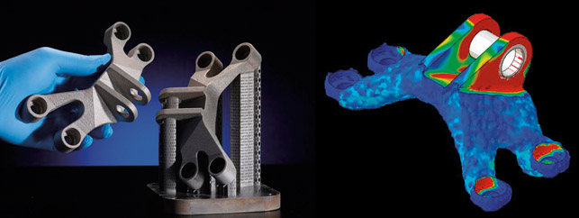
A selective laser melting (SLM) part designed using Tosca topology optimisation and produced using the SLM process
The design freedoms of the SLM process enable complex, lightweight parts with optimal material distributions to be produced (see image above) that could not otherwise be made using conventional manufacturing methods.
However, the extreme temperature cycles and rapid cooling rates that parts see during SLM processing tend to lead to unfavourable metallurgical structures, high residual stresses and undesirable levels of distortions (shape imperfections). In the worst-case scenario, the process-induced residual stresses can cause cracking during the build process, or the distortions may be so large as to cause damage to the wiper during re-coating. Hence, enhancing the as-manufactured quality of SLM parts is a major milestone to enabling the wide-scale adoption of SLM as a manufacturing process.
To address this challenge, TWI is undertaking validation activities, in collaboration with the Simulia brand of Dassault Systèmes, to improve the fundamental understanding of the SLM process.
Could finite element analysis (FEA) meet the challenge posed by additive manufacturing? Using new physics-based finite element method (FEM) formulations available in Abaqus 2017, London and his colleagues created heat transfer models of the process using Abaqus/Standard on a “double cantilever” test piece.
The new solution features enable the exact machine information about the powder recoating sequence, laser scan path, and process parameters to be directly input into the FE model.
These state-of-the-art capabilities enable progressive element activation, progressive heating computations and cooling of the evolving solid surface of the part as the build progresses.
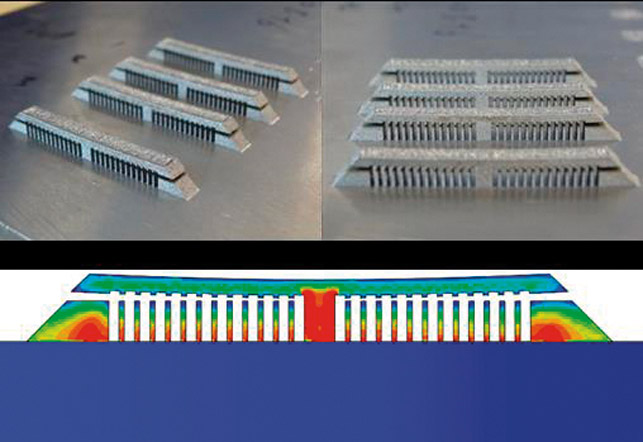
SLM double cantilever samples (top) and simulation (bottom)
“Using CAE, we created the CAD geometry and exported an STL file that we sent to the laser AM team. They then specified how they were going to build the part – layer thickness, laser power, scan strategy and so on,” says London. “This process information was used to construct the heat transfer model, which was then used to drive a mechanical model from which distortions and residual stresses were calculated.”
The double cantilevers themselves were then printed using Ti-6Al-4V powder with a Renishaw AM250 machine. After manufacturing the double cantilevers, TWI used wire electrical discharge machining to cut the support structures just below the solid beam surfaces. Upon cutting, the locked-in residual stresses generated deflections of the remaining beam structure. The out-of-plane deflections were measured and compared with the model predictions. Strong agreement between the predictions and measurements was observed leading to confidence in the use of this new modelling approach.
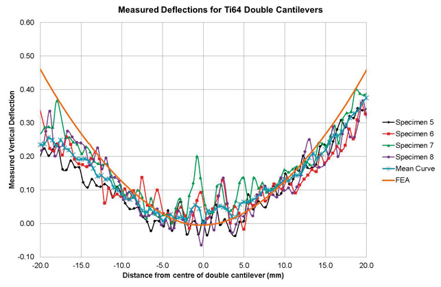
Comparison between experimental measurements and FEA predictions for cantilevers
Out of the powder bed: Electron beam wire-fed additive manufacturing
“While powder-based additive manufacturing techniques allow complex geometries to be fabricated, they are inherently slow processes,” says Nick Bagshaw, a consultant and simulation engineer in the Electron Beam group at TWI.
“Wire-fed additive processes enable a large volume of material to be deposited rapidly, but typically, a final machining or distortion correction operation is required to reach the final dimensional tolerances.”
However, this offers a significant reduction in material wastage compared to machining the final component from solid. High deposition rate processes have been associated with distortion and for industrial applications, it is important that distortion is minimsed.
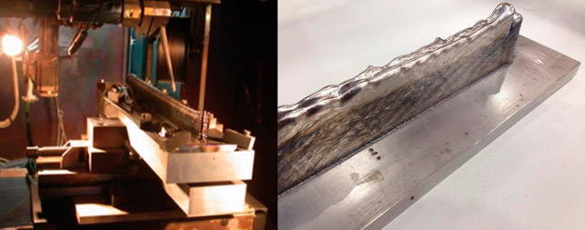
Wire EBAM test set-up (left) and an example of a W-EVAM test piece
To better understand the quality of Wire-Electron Beam Additive Manufacturing (W-EBAM) components and to help define the potential commercial application areas for W-EBAM, TWI simulated, built and measured Ti-6Al-4V parts built using the W-EBAM process.
Trials were conducted on a Hawker Siddeley Dynamics 6kW beam power EB welding machine. The machine is fitted with an in-chamber CNC controlled wire-feeder that is equipped to feed 1.6mm diameter wire. Bespoke tooling was developed and a clamping procedure defined to hold the plates during processing as shown in Figure 6.
A conventional welding simulation approach was used to model the W-EBAM process, leveraging the “model change” and element activation capabilities of Abaqus. Each 1.5mm layer comprised of two parallel passes; simulations were used to predict the thermal history and resulting distortion of structures ranging from 12 to 50mm high depositions.
The model was successfully validated across all ranges of build height investigated and the simulations were able to accurately capture the stiffening effect caused by the structure as its height increases.

Comparison of coordinate measuring machine (CMM) measurement (left) with FEA predictions from Abaqus (right)
Next steps
“Regardless of the AM process, we are looking into having robust and reliable means to predict temperature evolutions, distortion and residual stresses,” says London.
“Ultimately, we are looking to calibrate and validate metallurgical phase transformation models in the advanced process simulation capabilities in Abaqus so we can predict phase fractions, grain sizes and shapes, and the microstructural evolutions that occur during printing. The aim is to be able to predict the mechanical performance of AM parts.”
Validation work presented at the Science in the Age of Experience conference, which was organised by Dassault Systèmes and took place earlier this year in Chicago, shows that progress is being made. “The collaboration between TWI and Dassault Systèmes is helping us achieve the goal of having a comprehensive capability validated over the next few months,” concludes London.
TWI & Dassault Systèmes explore accurate predictions of additive manufacturing methods with Abaqus
Default


