How do you shift your business to take advantage of the clean energy movement? We talk to one company that has done just that and taken the solar power manufacturing market by storm
According to several reports, the Clean Tech industry is seeing a massive rebirth of investment now that the economic strife of the last few years is easing off.
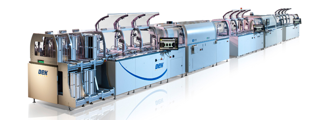
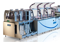
DEK Solar provides an agile production system that handles wafer printing and subsequent processes that can quickly be adapted to a customer’s requirements
According to Greenbiz.com’s annual Green Business Report, clean tech investments are up again this last year to just shy of the $4 billion mark. Amongst various ‘clean’ energy sources, solar is getting the biggest portion of that investment.
But although it may have filed the largest number of patents in the past few years, what about those manufacturers developing the infrastructure that is enabling companies to harness energy from the sun?
One such company is DEK Solar, which has grown out of DEK Printing Machines, a specialist in screen printing equipment. “We started to sell equipment to solar manufacturers over 25 years ago” says Darren Brown, DEK’s solar manager. “Of course, then it was just another thick film process – the printing of inks in relatively thick layers around 10 to 100s of microns onto various substrates.”
A future in solar?
With its knowledge of printing and automation, DEK soon realised it could take advantage of the clean tech revolution and in 2007 set up DEK Solar, a centre for engineering and manufacturing in Weymouth, UK. Once the viability for specialised solar cell manufacture equipment had been established, a small engineering team was assembled.
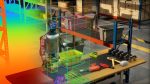
What’s surprising is the period of development: initial design, beta testing, production, to first customer was only 12 months using a combination of Pro/Engineer, Windchill PDMLink for document control, FastCAD (for wiring and harness design) and another system for change control. Chris Collinson, CAD systems administrator at DEK, believes that DEK’s data is usually around 4,000 unique parts, but once instances are included, that part count gets into the region of 6,000 assembled components.
DEK’s solar cell lines are modular, allowing the sales engineers to adapt a modular range of sub-systems to suit the customer’s requirements. “It’s a dedicated equipment set, but within that equipment set it’s pretty configurable,” says Brown. “Our SMT (Surface Mounted Technology) equipment can be likened to a Swiss army knife, it will print onto substrates from a couple of inches square to a couple of feet and you can print any multitude of materials. With the solar equipment, you would liken it more to a scalpel as is designed specifically for that purpose only.”
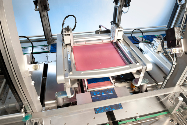
The portion of the solar cell manufacturing process that DEK covers focuses on the latter stages of the process, utilising silicon wafers (typically either 125mm or 156mm square and between 120 to 220 microns thick). Challenges in the design process relate to the fragile nature of the crystalline silicon and material handling in general.
According to Brown, production rates are a key focus.
“There are technical challenges relating to the way we handle these substrates,” he says. “The drivers for the industry have traditionally been through put, so the operational speed and capacity of the line as well as the handling of thinner substrates are key as they determine actual end of line yield.”
Brown explained that breakage is a massive concern. “You’re trying to process a piece of silicon that’s 180 microns thick (essentially a large piece of eggshell) at anywhere between 1,200 to 3,600 wafers per hour. So, one part is being processed every one to three seconds.
“The screen printing process itself is a contact process with pressure being applied to these wafers. Although you’re going for speed, you’re handling eggshells. If one breaks, it’s not just a case of a corner chipping off, they tend to shatter into multiple fragments. This will often bring the line down and then you’ll have to clean it down and recover as quickly as possible.
That’s one of the areas we’re putting a lot of work into – recovery times. It’s all well and good having a line that’s running at 3,000 parts per hour, but if every time you break a cell it took up to 30 minutes to get it back up and running again, you’re wasting your time. Typical breakage rates on these lines are less than 0.2 per cent, which sounds low but not if you’re running 3,000 cells per hour,” he adds.
As DEK’s equipment is at the end of a process chain the cells have already been through multiple production processes. These processes can introduce a lot of stresses into the wafers and could have caused micro cracks, which will always give rise to a certain level of breakage.
Silicon shifts
Another key challenge for DEK is the move away from mono-crystalline silicon. As Brown explains, the demand for mono-crystalline silicon was consumed by the chip making industry resulting in a serious shortage several years ago. This prompted the move to polycrystalline silicon.
“Poly-crystalline means that instead of growing a single crystal and slicing it up, they pour the molten silicon into the mould and it forms many crystals,” says Brown. “You can liken Monocrystal to a nice piece of mahogany and Polycrystalline to chipboard. Because the wafer has been sliced from a block of silicon made up of many different crystals, you get grain boundaries between them, which are basically faults. The handling challenges have increased as manufacturers have switched to the polycrystalline wafers.”
However, has this change in materials had an effect on the efficiency of the cells? According to Brown, there has been a minor trade off on efficiency. A good mono-cell can be up around 18 to 19 per cent efficient, while a poly-cell can be around 16 to 17 per cent So, there is a couple of percentage points in efficiency as a trade off, but that’s counted by lower cost of the silicon itself and availability, “ he comments.
A bright clean future
Now that the silicon foundries geared towards poly-crystalline silicon have been established for a couple of years, the supply rates are much better. With a combination of expert knowledge in both this field and the screen print industry as a whole, DEK has been able to take advantage of the burgeoning interest and investment in solar power.
But it can’t rest on its laurels. As Collinson comments, “One of the biggest design challenges we had was making the production lines modular. In the early days, the customer would specify what they wanted so we would need to modify or design that module to suit. Now we’ve got a wide range of modules designed that most customers can select from. That’s one of the biggest challenges, meeting the customers requirements at the speed they want it.”
www.deksolar.com
The sun shines for DEK Solar
No
Default