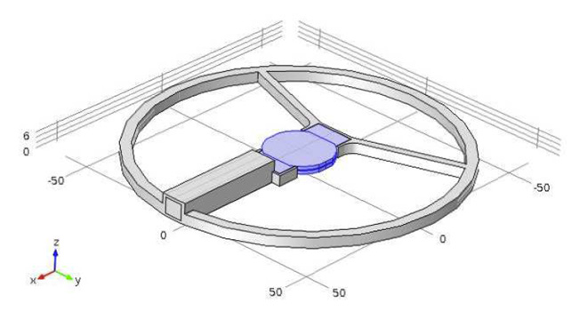
Fig 1: Geometry of the embedded structural health monitoring sensor, with the sensing part highlighted in blue
For specialists who design microdevices such as actuators, controllers, drivers, sensors and transmitters, growing demand for miniaturised electronics and Internet of Things (IoT) devices is creating new challenges.
From responsive equipment and wearable monitors to energy-efficient lighting in the office and automation on the factory floor, engineers need to bridge the gap between their microscopic semiconductor components and our macroscopic world with reliable and innovative products.
This is inspiring them to explore new ideas in the virtual world of numerical simulation.
STMicroelectronics, a world leader in designing and manufacturing semiconductor solutions, employs 7,500 individuals in the area of research and development (R&D).
According to Lucia Zullino, a technology R&D engineer at the company: “In our field, we need to analyse very small structures and understand their interaction with large packages in different configurations over a wide range of environments and applications.”
For semiconductor manufacturers like STMicroelectronics, the choices that engineers make in terms of materials and design are critical – and simulation plays an important role in evaluating materials and performance parameters.
“Much of our work is done through the Comsol Multiphysics software, which we use to validate hypotheses and to optimise products,” explains Zullino.
“There are about 30 users within STMicroelectronics, and although we belong to different departments and work in various locations, we are continually building and sharing knowledge about mathematical modeling techniques used in several projects.”

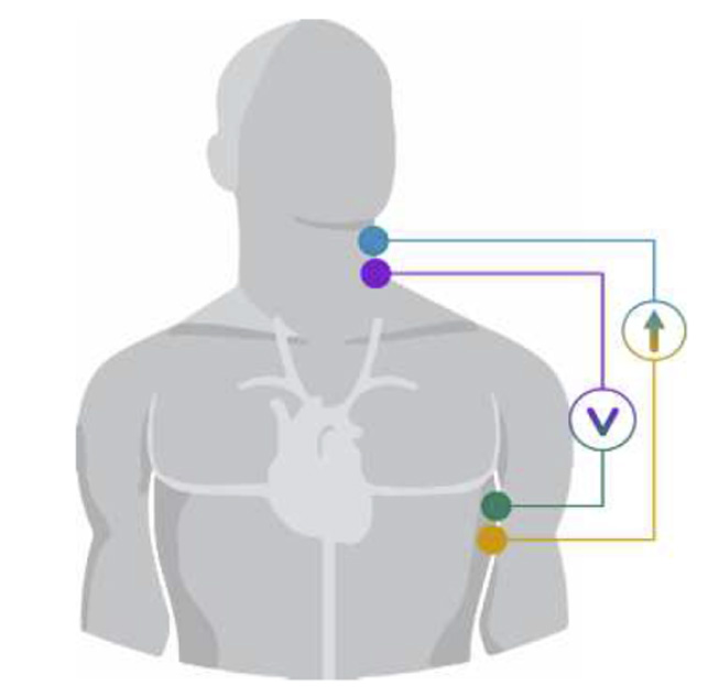
Fig 2: Technique used to measure the bioimpedance of an organ
STMicroelectronics – Understanding interactions
Simulation is used to understand multiphysics interactions at every stage of the development process for several of the company’s products.
Examples include optimising an epitaxial reactor for faster wafer production; controlling reactant flow distortion in the wet etching process; and investigating the interaction between die and package at the microscopic level.
In addition to design and manufacturing of microchips, engineers at STMicroelectronics work on the design of miniaturised actuators such as micromirrors used in recognition technologies that require optics and cameras.
Simulation was also used in another actuator-related project to investigate printheads and compare the effectiveness of two different working principles: displacement of ink through pressure-generated bubbles or using a membrane actuated by a PZT, a ceramic material made of lead zirconate titanate.
Through this work, the researchers were able to determine that the thin-film piezo printhead offers better compatibility with a wide variety of inks, higher printing speeds, superior print output quality and extended printhead lifetime.

Fig 3: A 3D model created from computed tomography (CT) images (left), postprocessed with CAD tools (middle), and then interpolated to generate the volumes (right) needed for the analysis
In yet another development project at STMicroelectronics, simulation was used to analyse the properties of concrete and to predict the capacity of an embedded sensor (figure 1) to monitor age-related changes and relay a signal to the surface.
This structural health monitoring (SHM) system has already been deployed in various locations in Italy. Here, it is being used on various built structures, in order to assess the health of the concrete from which they are constructed and to log any damage that the structure incurs when it is exposed to unexpected stress.
In this way, the SHM system enables engineers to keep a close eye on structural integrity and reliability of infrastructure.

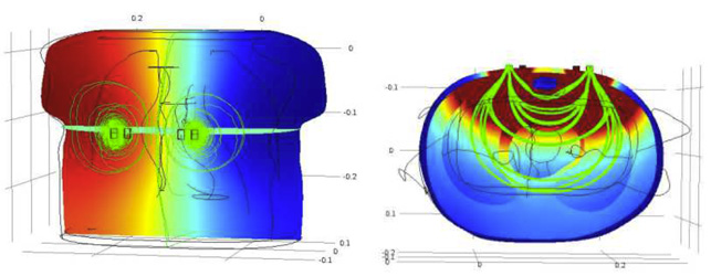
Fig 4: Simulation results showing the electric voltage and current distribution in a human torso
Wearables for health
Over the years, STMicroelectronics has developed many healthcare applications. In one prototype project, a patch was designed to measure the bioimpedance of an organ, such as the heart, inside the human body (as seen in
figure 2).
Working from medical imaging of human organs, researchers created a 3D model (figure 3) to run an AC/DC simulation in the frequency domain (figure 4) and assess the effect of the electrode shape and position on the measured physiological parameters.
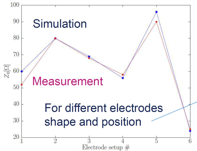
The simulation results they obtained (figure 5) correlated closely with real-life measurements and enabled the development of a wearable configurable patch, capable of indicating physiological changes.
These sensors will enable doctors and other healthcare workers responsible for monitoring various heart conditions to get real-time data to provide patients with the best care, using the latest technology.
“Through simulation, we have learned a lot about potential problems and we have gotten better at optimising semiconductors for the outside world,” says Zullino.
“Simulation now drives product design, both for internal and external customers.”

Fig 5: Comparison between measured and simulated bioimpedance values

Fig 6: for different electrode shapes and positions
She and her colleagues see many other opportunities to use multiphysics simulation in other aspects of development. For example, she says, studies on humidity levels inside packaging and the potential for corrosion are already in progress.
“We can assess materials and structures more quickly and screen for the best ones, which means less time spent on trials, better technical decisions and quicker business decisions,” she says.
“Compared to physical testing, we can implement new solutions and verify them at zero cost. Simulation is one of the key tools that drives innovation.”


