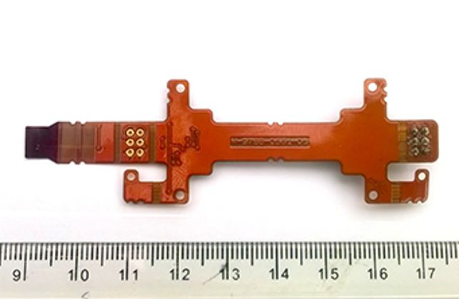
Designed recently for a new encoder, the flexible PCB is about 8cm long
Flexible and flexi-rigid Printed Circuit Board Assemblies (PCBAs) are integral components within many of Renishaw’s metrology instruments. However, flexi-rigid PCBAs in particular can be a challenging proposition from a design perspective as they can include several rigid PCBAs and typically need to wrap around – or fit within – complex and volume constrained mechanical assemblies. Such flexi-rigids tend to be non-dynamic, ‘fit-once’ PCBAs.
In other cases, flexible PCBAs or ‘flexis’ are needed to establish electrical connections between parts of the instrument that move relative to one another. They need to be dynamic and flex frequently whilst the instrument is working.
Historically, the design of flexis and flexi-rigid PCBAs has been a predominantly 2D exercise for Renishaw’s PCB designers. They would accept a 2D board outline from the mechanical designer engineers (working in 3D) and – following PCB place and route – return the design with skyline information to the mechanical engineers, who then fold the flexi/flexi-rigid PCB in their 3D environment.
However, since migrating to Zuken’s Design Gateway and Design Force, tools within Zuken’s CR-8000 PCB design platform, Renishaw’s PCB designers can now work in 3D.
Renishaw has been using Zuken products since 2000, and in 2016 the company made the decision to migrate from System Designer and Board Designer (tools within Zuken’s CR-5000 platform) to Design Gateway and Design Force, tools within Zuken’s CR-8000 advanced EDA design platform, for schematic capture and PCB layout respectively.
A major benefit of the migration to CR-8000 is that Renishaw’s PCB designers have the ability to visualise and manipulate board designs in 3D. “We can place components in a 3D environment, taking into account any constraints that may have come over from our mechanical engineers, and then switch back to 2D for routing,” says Pete Leonard, electronic design manager for Group Engineering at Renishaw.
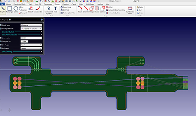
The flexible PCB or ‘flexi’ is required to bend in several places
3D visualisation
The ability to work in 3D is particularly useful for Renishaw’s PCB designers when considering flexible and flexi-rigid PCBs; a task the company has to perform throughout the year to support new product introductions.
In the design of the flexible PCB, Renishaw’s designers created a user-defined layer called ‘BendLine’ (a casesensitive reserved name). On this BendLine layer, polylines were drawn to represent the axes around which the flexible PCB needs to bend.
Properties such as bend direction, angle and radius were then applied to each of the polylines.
Renishaw’s PCB designers were then able to move components around in this 3D environment. They were also able to import (via a .stp file) the housing around which the flexible PCB must bend.
“Historically our PCB designers have not had sight of the housing in their design environment,” adds Leonard.
“Now they can visualise how it all fits and both they and our mechanical design engineers can see if any clashes occur.
This allows us to identify and fix any integration issues early on in the development lifecycle – which is when they are easier and less costly to fix.”
It is also anticipated that Renishaw’s PCB designers will soon be exporting .stp files to the mechanical design engineers. Leonard continues: “They’ll be able see the orientations, locations and sizes of mounted components.
They’d also have the authority to position certain features, such as voids, in the housing that may aid the PCB designers with component placements.”
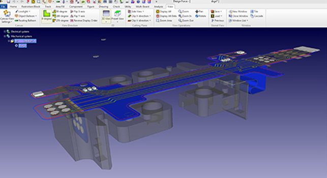
The flexi design wrapped around the housing
Controlled impedance
The ability to work in a 3D environment is also helping Renishaw’s PCB designers construct controlled impedance flexible circuits.“Controlled impedance routing is a prerequisite for good digital circuit signal integrity, and signals – particularly high frequency ones – require constant characteristic impedance from driver to receiver,” says Adrian Welsford, Renishaw’s principal design engineer for signal integrity.
The impedance of a flexible PCB’s track is derived from the ratio of its inductance and capacitance, properties which are themselves derived from conductor dimensions, the space between conductors and the strength of the electric and magnetic fields surrounding the wire/track. To this end, Renishaw’s PCB designers can employ the field solvers within Design Force.
For non-dynamic flexible PCBs requiring controlled impedance tracks, these are formed by sandwiching tracks and a ground plane between layers of polyimide.
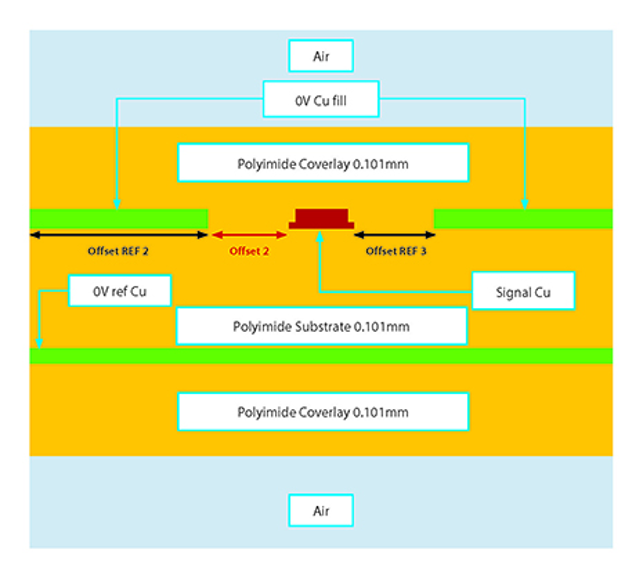
The cross section of a non-dynamic flexible PCB. A bend neutral axis runs through the centre of the substrate (not shown)
In the image above, the polyimide substrate between the reference plane (0V ref Cu) and the signal track (Signal Cu) can be thought of as the dielectric layer of a capacitor. Also taken into account by the solvers within Design Force are the polyimide top coverlay and the air above, as anything below the reference plane (0V ref Cu) can be ignored. Subject to their proximity, the copper fills (0V Cu fill) may also need to be included within the solver’s calculations.
“As the flexi bends the copper tracks and reference plane will be subjected to forces of compression or tension,” explains Welsford. “Our PCB designers therefore endeavour to leave as much copper on the routing (signal track) layer as possible to ensure the compression and tension forces are equal, thus minimising the risk of inner conductor creasing. Also, there’s an advantage in having fairly thick copper tracks, fills and planes if the non-dynamic flexi is to maintain its profile without support once it’s bent.”
For dynamic flexible PCBs, only a single layer of copper is allowed (see image below). Also, in order to assure a long flex life through reduced bend stress, the copper tracks and fills need to be thin. However, in reducing the thickness of signal tracks it is frequently necessary to increase their widths; and it can soon become difficult to maintain gaps between tracks to ensure a 50 Ohm impedance.
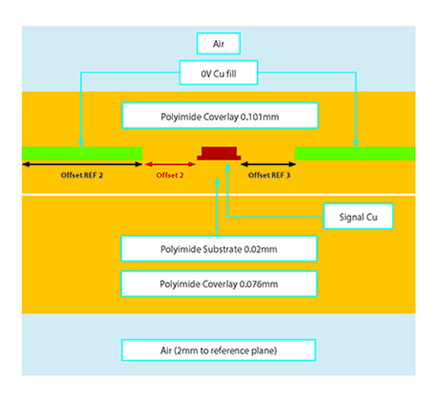
The cross section of a dynamic flexible PCB. The bend neutral axis will ideally run through the centre of the copper layer
Welsford adds: “In some instances it is necessary to design the flexi with higher than normal track impedances and to adjust rigid PCB tracks, drivers and receivers by way of impedance matching.”
Renishaw is currently using two tools from Zuken’s CR-5000 suite for controlling impedance. Constraint Manager is used to specify the limits of characteristic impedance and Lightning is used to create impedance templates.
“This allows us to select a group of nets, using a net class, and then use the field solver to automatically calculate the impedance specified – adjusting the track widths to match,” explains Welsford. He adds that Renishaw plans to start using tools within the CR-8000 suite for impedance control.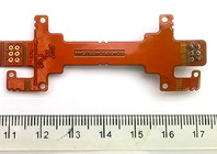
Collaboration at Renishaw thanks to Zuken
Default


