With AMD Solid State Graphics (SSG), which looks set to come of age with Vega, users can explore huge viz datasets in real time – such as this 600GB physically-based rendered architectural interior scene.
AMD is starting to give some clues as to how its next generation Vega GPU architecture might benefit design, engineering and architecture firms – beyond the givens of real time visualisation, Virtual Reality (VR) and static physically-based rendering.
Much of this appears to hinge on Vega’s re-architected memory architecture, which gives the GPU the ability to access Terabytes of virtual address space through a high-bandwidth cache controller.
At the recent AMD Technology Summit in California, AMD showed a raw tech demo of an architectural interior scene where the user could navigate freely around the space.
This wasn’t a ‘game engine’ experience based on OpenGL or DirectX. It was a ‘photorealistic’ environment that had been pre-rendered with AMD’s physically-based rendering technology, Radeon ProRender.
Ray-tracing with any physically-based renderer is hugely compute intensive and a single image can take hours to refine, even on a very powerful GPU.
For the live demo, the workstation’s GPU wasn’t ray tracing in real time (AMD pre-rendered the equivalent of 1,000 frames using multiple GPUs) Instead it was working hard to construct the view as the user navigated the scene.
This looks very similar to what Nvidia is doing with Iray VR (interactive photorealism, albeit in Virtual Reality).
The interesting thing about AMD’s demo was the size of the dataset and where it was stored in relation to the GPU. A total of 600GB was being streamed in and out of GPU memory from the GPU’s on-board Solid State Drive (SSD).
AMD has dubbed this on-board SSD, Solid State Graphics (SSG). And because the SSG is right next to the GPU, data moves very fast – at a rate of 5GB/sec, according to AMD’s Takahiro Harada.
A traditional GPU’s memory currently maxes out at 32GB, so bigger datasets must be streamed on demand over the PCIe bus, read from the workstation’s SSD or system memory, via the CPU.
It was only by using the SSG as a fast buffer between system storage and GPU memory that AMD was able to deliver this physically-based rendering experience in real time. Without the buffer, the area of navigable floor space would have been much smaller – or there would likely have been significant pauses as fresh data was loaded up to the GPU.
AMD’s technology demonstration was far from polished. Harada admitted that he only had two days to prepare the demo, which was not enough time to fully render the images so they were left unresolved and quite grainy. There was also some lag on navigation (nowhere near the 30+ FPS you expect from a game engine experience) but AMD was keen to point out this was an early research project, rather than a product.
While the demo focused on architecture, Harada agreed that this technology would also be very relevant to other sectors such as automotive. Currently, firms carry out interactive design review with OpenGL-based applications such as Autodesk VRED, which approximates lighting, reflections and shadows, albeit in a very convincing way.
With physically-based rendering, because light is simulated, rendered images should more accurately represent objects as they would appear in the real world.

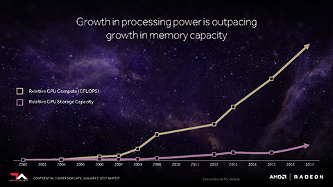
AMD believes that Vega will help GPU memory capacity keep pace with processing power.

Thanks to its new high-bandwidth cache controller, Vega will be able to access up to 512TB of virtual address space
AMD first announced its SSG technology (Radeon Pro SSG) at Siggraph in August 2016. This first technology preview was based on AMD’s Fiji architecture, but it looks like Vega will take SSG to a whole new level.
With Fiji, for ISVs (Independent Software Vendors) to bind data on the SSG, custom code would need to be written to make calls to OpenCL extensions, OpenGL extensions or DirectX extensions.
With Vega it sounds like software will be able to take advantage of the Radeon Pro SSG without having to change code, as Raja Koduri, senior vice president and chief architect, Radeon Technologies Group, AMD, told DEVELOP3D.
“In Vega because of the high-bandwidth cache, and the controller we have, we can provide transference mechanisms,” said Koduri. “The ISV doesn’t really need to do anything. We can map SSG memory directly to the high-bandwidth cache and move data directly between them.”
This could have huge implications for GPU compute, particularly in simulation (CAE). Traditionally, when using the GPU to solve FEA or CFD problems the CPU has to break down jobs into bite sized chunks that can be loaded into GPU memory.
With SSG, it sounds like it would be possible for one GPU to solve extremely large problems.
This would mean AMD’s stated vision from a few years back of being able to simulate on a single node, could come to fruition.
In 2015 AMD also broke down some barriers for its GPUs to be adopted for GPU compute. As part of its Boltzmann Initiative, AMD made it easier for software developers to convert applications written in C for CUDA (which only run on Nvidia GPUs) into OpenCL (the open compute standard, supported by AMD and other vendors).
In theory this means firms like Ansys, who have a made a large investment in CUDA, could easily port code to OpenCL to take advantage of the ‘Vega’ Radeon Pro SSG and its ability to work with huge engineering datasets.
If that is the case then AMD could make a much bigger impact in a niche market that has traditionally been dominated by Nvidia.
AMD is due to launch Radeon Pro professional GPUs based on Vega in 2017. It has already announced the AMD Radeon Instinct MI25 accelerator, a passively cooled server GPU for deep learning, which should deliver an expected 25 TFLOPS of peak FP16 (half precision) performance, which is similar to that of the Nvidia Quadro P6000. For peak FP32 (single precision) we expect this to be 12.5 TFLOPS.


